28+ Arduino Uno R3 Pcb Layout
Photos. Vaibhav.happy to share one more best design of my pcb work, that is arduino uno r3 custom we all knew that pcb editor is what ultimately we need, we have schematic means we need to convert it into pcb layout which is done by pcb editor. In our last two posts, we focused on the software aspects of the arduino.
Arduino Uno Eagle Blocksfasr from www.eng.uwaterloo.ca
The arduino uno pinout guide includes information you need about the different pins of the arduino uno microcontroller and their uses: The attached 80x45mm lcd dominates the surface there are cutouts placed in the pcb where the arduino's power supply and usb connector are located because these parts protrude upwards just. This decreases parasitic capacitance and more importantly parasitic inductance which.
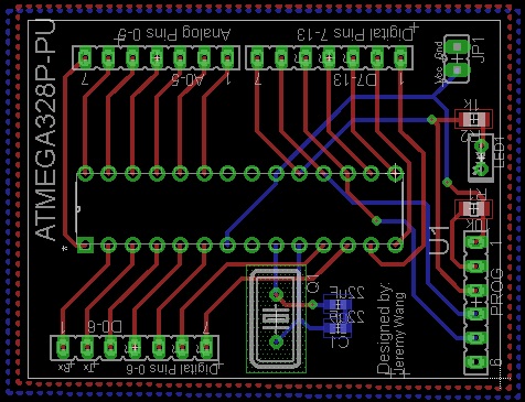
The pcb layout is all based around the restrictions of having to fit onto the arduino uno as a shield.
We saw that arduino boards are programmed. The pcb layout is all based around the restrictions of having to fit onto the arduino uno as a shield. This decreases parasitic capacitance and more importantly parasitic inductance which. Also what is the easiest way to output the arduino uno pcb files found on the main arduino site to gerber files?